Introduction
Both the Atomic Force Microscopy (AFM) and the Hall Effect represent unique methods of magnetic field measurements. While the AFM method employs a probe that is placed on its tip to take these measurements, Hall Effect explores ‘Hall’ voltage to achieve the same. These measurements come in handy in the characterization of semiconductor devices. Among them, there are other measurements like the resistivities, Hall coefficient and Hall mobility that can be obtained and are also vital in the characterization of the same. These measurements are also determined by the van der Pauw (vdP) geometry and they do also help in the selection of excellent material for a specific semiconductor.
With regards to AFM, there are more than a dozen scan-proximity-based microscopes. Nonetheless, they operate under the same principle to inspect a local property including the height and magnetism. The micro-separation between the probe and a sample enables the equipment to inspect a specific area, portraying an image of the sample. The image attained by this method takes after that obtained by a television set “in that both consists of many rows or lines of information placed one above the other” (Koo-Hyun, 2007). Of note, the efficiency of the equipment depends on the probe’s size rather than a system of lenses that are absent in its system. In view of the Hall Effect, this is a consequence of the Lorentz force that happens when a “current-carrying conductor is placed in a traverse magnetic field” (Koo-Hyun, 2007). This force results in the production of a voltage that cuts the magnetic flux at right angles. The presence of this voltage has a bearing on both the charge sign and density in a semiconductor.
In this report, we explore the science behind AFM and the principles involved in both the Hall Effect and the vdP techniques.
Atomic Force Microscopy
AFM is an important technique that is employed in nanotechnology research. In order to achieve its function, the AFM explores the surface topography. Nonetheless, its tip can effectively act as a probe in electronics to characterize materials at a nanoscale level. Such material properties as resistivities, capacitance and the superficial voltage (Pd) can easily be determined concurrently with topographic information. To this end, a novel equipment that is quite complex has been developed, requiring “the interplay of topographic and electrical information to quantify AFM-based electrical measurements at the nanoscale level” (Koo-Hyun, 2007). In spite of these complexities, this technique offers unique information vital in the electrical characterization of ever-contracting electronic devices like semiconductors. This equipment incorporates unique features like photosensitive diodes, a flexible cantilever, sharp tips, high resolution and a force feedback mechanism to achieve atomic-scale resolution.
In electric measurements, AFM employs a force probe on its tip to determine the magnitude of a force (repulsive/attractive) between it and the sample. In a repulsive (contact) mode, the AFM explores its tip (cantilever) to briefly touch the material under investigation. Consequently, a detection system records the sample’s local height courtesy of “the vertical deflection of the cantilever” (Koo-Hyun, 2007). On the other hand, the topographic images are obtained when the tip is in a non-contact mode. Unlike electron microscopes, “AFMs have the abilities to image material samples that are in the air and those submerged in liquids” (Koo-Hyun, 2007).
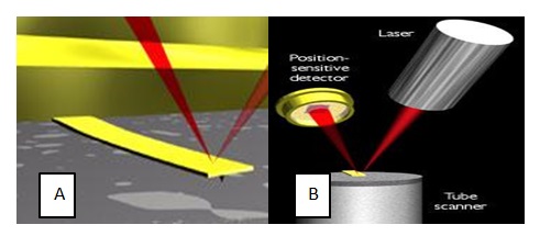
To obtain accurate data on the cantilever deflection, a laser beam is applied. To this end, the cantilever acts as a reflecting surface of a laser beam (fig. 1), with an angular deflection of the beam producing twice as much deflection as the original beam. This beam is detected by two photosensitive diodes which give information about the laser spot location and hence the cantilever’s angular deflection thanks to “the difference between the two photodiode signals” (Willemsen, 2000). Notably, since the size of the cantilever is minute vis-à-vis the cantilever-detector distance, the motions of the probe are significantly amplified by the lever.
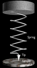
What makes AFM cantilevers efficient is that they possess a high flexible stylus (fig. 2) which exhibit high resonant frequency, making them highly responsive. This stylus, exhibiting a small Young’s Modulus (≈0.1N/m), offers no damage to the sample while scanning. The resonance frequency can be determined by the equation:
Resonance frequency = 1/2π√ (spring constant/mass).
As such, cantilevers come in small sizes and hence exhibit high resonance frequency (see the equation above). Their resolution is enhanced by sharp ultra clever tips.
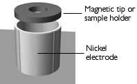
In an effort to achieve high resolution, AFM incorporates piezoceramics in its system to strategically position the tip/sample. Piezoelectric ceramics are unique kinds of materials that “expand or contract when in presence of a voltage gradient or, conversely, create a voltage gradient when forced to expand or contract” (Miller, 1988). One advantage of exploring piezoceramics is that it can achieve a three-dimensional positioning of a sample with enhanced precision. Contemporary AFM adopts tube-shaped piezoceramics in its system (fig. 3) to enhance its function.
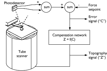
To control the force on the specimen, AFM explores a feedback mechanism shown in the figure below (fig. 4). The system incorporates “a tube scanner, an optical liver, a cantilever and a feedback circuit” (Binnig & Smith, 1986). While the roles of the first three components have been explained herein, the role of the feedback circuit is to steady the cantilever deflection thanks to the potential difference across the scanner. Of note, the speed at which an image can be acquired is dependent on the sensitivity of the feedback loop to steady the cantilever deflection. As such, the sensitivity of the feedback loop determines the performance of an AFM. To this end, efficient feedback loops operate at a frequency of approximately 10 kHz, acquiring an image within a minute.
Hall Effect
A current-carrying conductor placed inside a magnetic flux and cutting at right angles induces a potential difference between the edges of the conductor. This effect is what is referred to as the Hall Effect. The magnitude of both the current (i) and the magnetic flux (m) have an effect on the electric field intensity (e). To this end, the electric field intensity is directly proportional to m and i. Mathematically, this is represented as below:
e= kim, where k is the Hall Constant.
Of note, a conductor exhibiting Hall Effect portrays different polarities depending on the conductor’s atomic structure (Purcell, 2001).
Just like in conductors, semiconductors experience the Hall Effect. The degree of this effect on semiconductors is what is dubbed Hall Mobility. Mathematically, this is a product of k and the conductivity. Hall Mobility comes in handy when choosing a suitable semiconductor device for Hall generator, equipment used in the determination of the magnetic field intensity (Whittle, 1973).
Technically, when a semiconductor is exhibiting Hall Effect, the holes shift to the P-type section (fig 5).
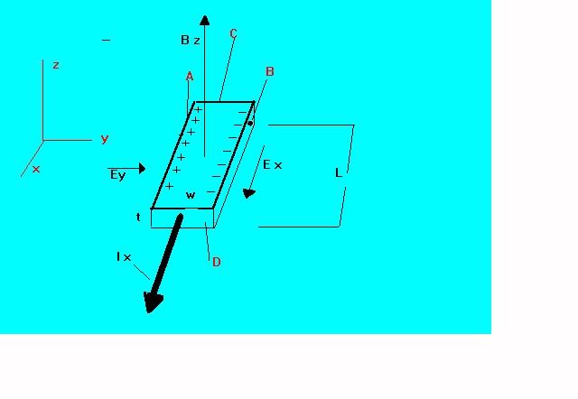
When considering the vector notation with respect to the motion of the hole we get:
F = q (E + VxB)…………………………….. (1).
Along the y axis, the equation below is obtained:
Fy = q (Ey -VxBx)…………………………. (2).
Theoretically, equation 2 means that the hole will move along the length of the bar only when a force due to the field (qEy) is established along the width of the bar. Otherwise, the hole will move in the –y-direction with a net force of qVxBx. Principally, at the moment the holes start drifting along the bar, Ey = VxBz. As such, there is no net backward force. This Ey is what is termed the Hall Effect. The ultimate voltage built i.e. VAB = Eyw is what is termed the Hall Voltage. To this end, the Ey is represented as below:
Ey = RHJxBz
(Tolansky, 1970).
In that respect, RH, J and B represent the Hall constant, density of the holes and the field respectively. The Hall constant is represented as below:
RH = 1/qpo, where po and q represent the density of the holes and the positive charge respectively.
Equally, when dealing with an N-type semiconductor, the same approach is applied.
The figure below shows an integrated circuit vital for Hall Effect measurements.
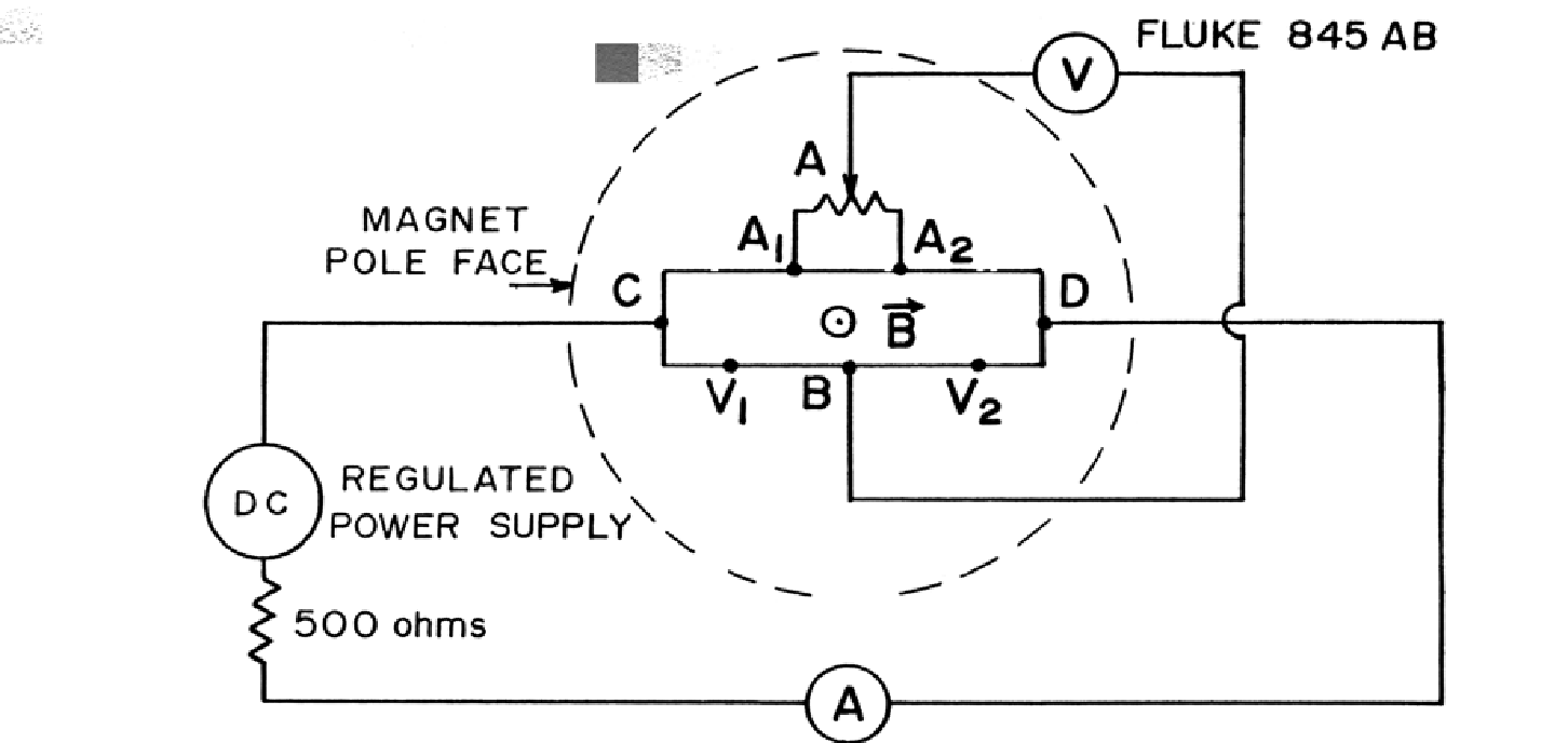
The Hall Effect can be used to study the correlation between majority charge carriers/mobility and temperature, a vital component in semiconductor characterization. Moreover, this effect comes in handy in the study of the magnetic fields in integrated circuit devices.
Van der Pauw (vdP) geometry
Van der Pauw geometry is a technique synonymous with the study of Hall coefficients and resistivities in semiconductor devices. Importantly, it should be noted that this technique as applied in Hall measurements is only applicable where there is no magnetic field influence. In addition to “the Hall contribution, measurements in a finite magnetic field generally include a term associated with field-induced changes in the longitudinal resistivity” (Van der Pauw, 1958). However, this can easily be eliminated thanks to the difference in field measurements taken at the opposite ends of the field. With respect to the resistivity measurements, vdF technique offers solutions to the problems experienced in conventional methods of resistivity measurements. Such a problem as imprecise placement of a specimen due to lack of knowledge about a sample’s geometry is eliminated. Also, the charge density should be evenly distributed across the cross-section at any one given point. In this report, we dwell much on the principle adopted by vdF in resistivity measurements.
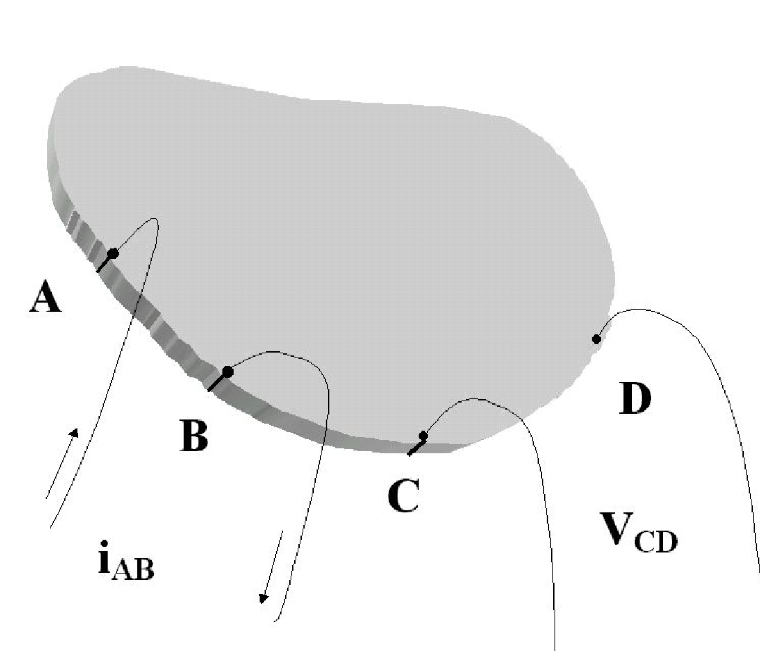
VdF technique was initially designed to take resistivity measurements in “thin and flat semiconductor samples” (Van der Pauw, 1958). Later, van der Pauw showed that this technique can be explored in the analysis of irregular-shaped samples with a parameter like the direction of the current not necessary. To this end, for this to be true, the following conditions are to be obeyed. First, the contact ought to be placed on the edges of the specimen. In this respect, if the specimen is not tiny in size, then the structure appears like a group of vertical lines stuck together across the entire length. As for the equipotential surfaces, the specimen is assumed to be cylindrical. Second, the contacts are to be reasonably small. Third, the sample’s thickness ought to be uniform. Finally, the sample ought to be continuous (without disjoining).
Some of these conditions are tasking and hence cannot be done experimentally. As such, finite “size of the contacts and of their erroneous placement was calculated in the case of samples with different shapes (fig. 7)” (Van der Pauw, 1958). To this end, the following equation was derived:
exp (-πRAB, CDd/ρ) + exp (-πRBC,ADd/ρ) = 1,
Where RAB, CD = (VD-VC)/iAB, and iAB is the current in the direction AB.
An explicit equation “for the measurement of this parameter can be obtained on conditions that a sample contains a line of symmetry where contacts A and C are placed and that B and D are placed such that they are symmetrical relative to the axis” (Van der Pauw, 1958). To this end, the below equation on resistivity measurement was derived:
ρ = πd/ln 2 (RAB, CD).
Conclusion
In a conclusion, as it has been depicted in the above report, all the three techniques are designed to basically measure parameters that are basically related. While the AFM method employs a probe that is placed on its tip to take magnetic field measurements, Hall Effect explores ‘Hall’ voltage to achieve the same. These measurements are vital in the characterization of semiconductors. Between them, such measurements as resistivities, Hall mobility and Hall coefficient which differentiate different material samples of semiconductors can be obtained. On the other hand, the van der Pauw geometry presents a novel technique that is more efficient in the measurement of resistivities.
References
Binnig, G., & Smith, D. (1986). “Single-tube three-dimensional scanner for scanning tunneling microscopy”. Review of Scientific Instruments 57 (8), 1687-1688.
Halliday, D. (1962). Physics. New York, NY: Wiley and Sons Press.
Jenkins, F. (1957). Fundamentals of Optics. New York: McGraw-Hall Press.
Koo-Hyun, C. (2007). “Wear characteristics of diamond-coated atomic force microscope probe”. Ultramicroscopy, 108 (1), 1-10.
Miller, G. (1988). “Scanning tunneling and atomic force microscopy combined.” Applied Physics Letters, 52 (26), 2233-2235.
Purcell, M. (2001). Electricity and Magnetism. New York, NY: New York University Press.
Tolansky, S. (1970). Multiple Beam Interferometry of Surfaces and Films. New York, NY: New York University Press
Van der Pauw, J. (1958). “A Method of Measuring Specific Resistivity and Hall Effect of Discs of Arbitrary Shape.” Philips Research Reports, 12 (1), 1-9.
Whittle, Y. (1973). Experimental Physics for Students. London: Chapman & Hall Press.
Willemsen, O. (2000). “Biomolecular Interactions Measured by Atomic Force Microscopy” Biophysical Journal, 79 (6), 3267-3281.