Most of the electronic systems contain amplifier as a major component. The major function of the amplifier is to boost up the weak signal into a strong signal suitable for transmission. The transistor acts as an amplifier when it is in active region, that is, emitter base junction is forward biased and collector base junction is reverse biased. A single stage amplifier circuit is shown below.
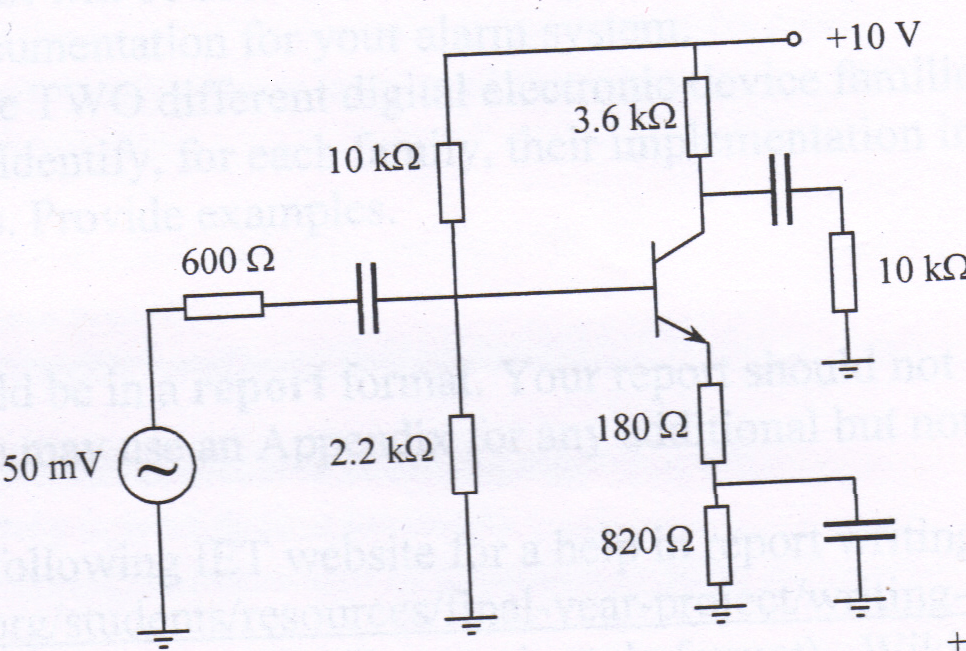
In order to provide better stability in the operating point, voltage divider bias is used. Since this circuit is used for AC application, additional capacitors are added along with this voltage divider bias circuit. The coupling capacitor or bypass capacitor passes AC signals and it also blocks DC; hence, the name blocking capacitor. The coupling capacitor is connected between the collector and the output of the circuit which helps the output across the10k resistor free from the collector’s DC voltage. Here, the capacitor connecting across the 820ohm resistor is known as bypass capacitor, because it passes all the AC current from emitter to the ground.
If we are not connecting that coupling capacitor to this circuit, if any AC voltage is developed across the resistor, 820ohm will affect the input signal, that is, 50mv. Such kind of AC feedback is eliminated by using this bypass capacitor across 820ohm resistor. If it is useful for effective bypass to low frequency signals, its performance is enhanced in high frequency signal. So, we have to select the value of the capacitor in such a way that it will have low impedance when compared to the value of the resistor which is connected at the emitter of the transistor at the lowest frequency present at the input level. Here it is 820ohm. That is, always select the reactance of the capacitor such that its value is always less than one tenth of the value of the resistance at the emitter side.
That is XCE<=RE/10
Here, the value of the output resistance is 10k.This output resistance of the single stage amplifier acts as an input of multistage amplifier. The voltage gain is the ratio of the AC voltage at the output and the input. Voltage gain is represented by Av i. e. Av=Vo/Vi
The output of the single stage amplifier is not in phase. The input and output are out of phase by 180 degree. This happens because when we increase the value of the input signal, the current at the base increases. This will cause the shifting of Q point lead to increase the value of collector current but to decrease collector emitter voltage.
Two stage RC Coupled Amplifier
Two stage RC coupled amplifier is mainly used in audio frequency applications.
The collector current of common emitter amplifier is controlled by base current.
A small increase in base current results in a large increase in collector current. Similarly, a small decrease in base current results in a large decrease in collector current.
The two stage amplifier can have both negative and positive feedbacks. The feedback can be adjusted and even the amplifier can be oscillated with the feedback. The biasing of each of the stage is facilitated by the isolation of DC at different stages.
A two stage RC coupled amplifier is shown below.
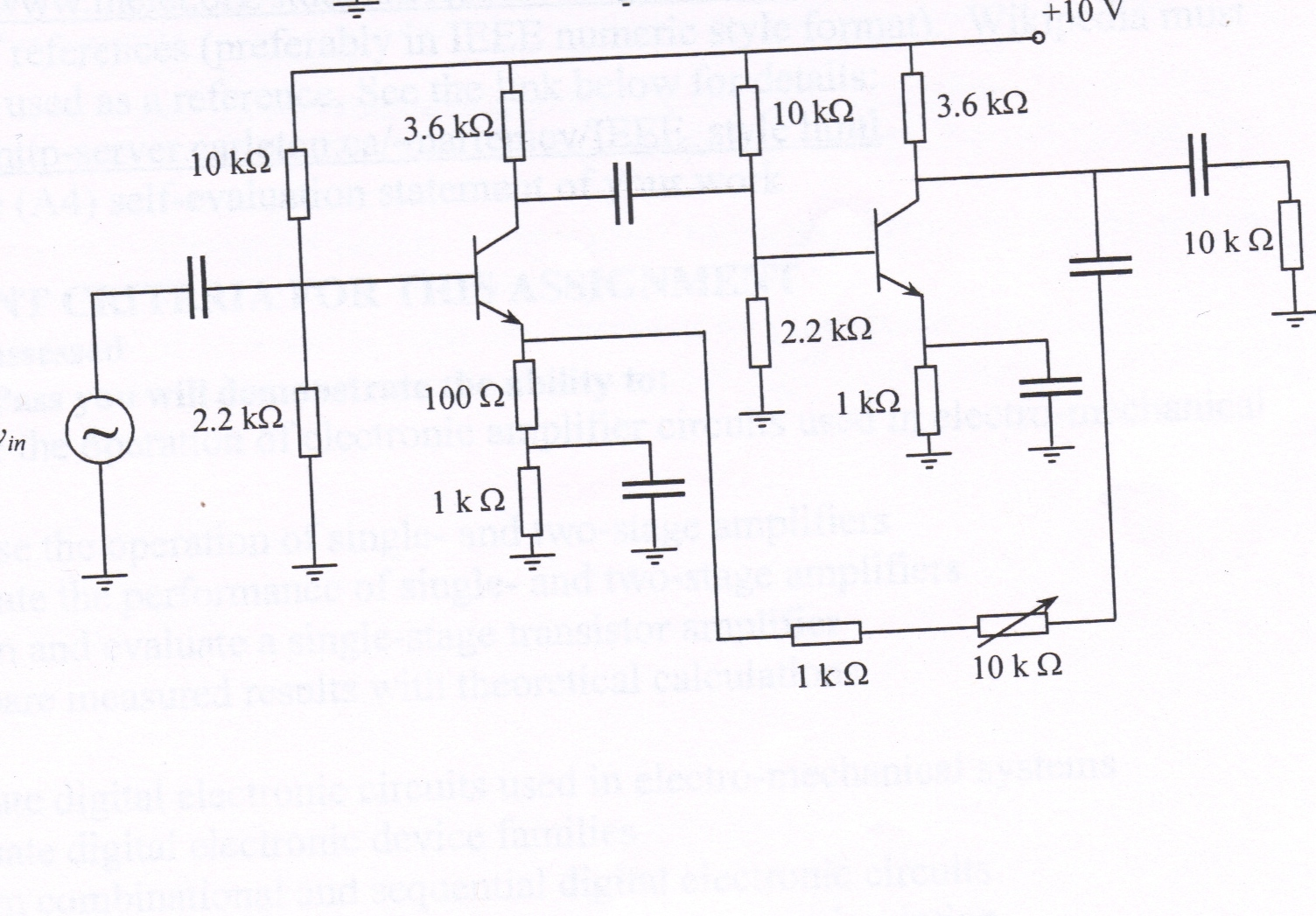
The gain of a single stage amplifier can be increased by cascading two or more amplifier stages. “In the single stage amplifier circuit a phase inversion of 180 takes place at each stage, hence the input & output at second stage will have the phase difference of 360 or they are in phase.” (Educational kits: Amplifiers: Two stages RC coupled amplifier).
The signal developed across the collector resistor of the first amplifier is taken to the base of the second stage through a capacitor. The coupling capacitor or bypass capacitor passes AC signals and it also blocks DC to the base of the second stage; hence the name blocking capacitor. Hence, DC biasing of the second stage is uninterrupted. The loss of amplification is also prevented by the bypass capacitor. Coupling capacitor results in the reduction of gain at very low frequency.
The amplifier response is also influenced by the blocking capacitor. The circuit also uses biasing resistors. The capacitor connecting across the 820ohm resistor is known as bypass capacitor. Normally, single resistor (1k) in parallel with a capacitor is used to compensate as well as to obtain desired frequency stability and response. If an additional resistor (100ohm) is used as shown in the above figure, it will cause reduction in the capacitive effect, and hence reduce the compensation. We can obtain the same effect by reducing the value of that capacitor without using the additional series resistance. Due to negative feedback, reduction in gain occurs across the emitter resistors.
This loss of gain can be prevented by the bypass capacitors. The resistors 10k, 2.2k and 1k are used in the circuit for biasing of the two transistors in the circuit. The selection of the resistors is in such a way that the operating points of the transistors lie on the centre of the particular DC load line for getting undistorted output waveform. The parallel combination of resistors 3.6k at the first stage and 10k at the second stage work as an AC load for the first stage and at the second stage the 3.6k at the collector alone acts as an AC load.
When feedback is connected in the two stages RC coupled amplifier, the gain decreases. Here, negative feedback is used in the circuit. Negative feedback means feedback energy is 180 degree out of phase with the input signal. In negative feedback, the gain of the amplifier decreases and stability increases. That is, in negative feedback, noise and distortion also decrease. In the two stage amplifier, an AC signal is given to the input of the first stage. The first stage transistor amplifies this signal and it reaches the collector resistor. Through the coupling capacitor this amplified output signal is then given to the input of the second stage which again amplifies the signal. Thus, amplification is done at two stages of the amplifier. So, the amplification of the output signal will be twice that of the input signal.
The advantages of two stages RC coupled amplifier over single stage RC coupled amplifier are the following.
- It is less expensive because it requires only low cost components, such as, resistors and capacitors.
- Frequency distortion is less and frequency response is large.
- It has a uniform bandwidth over wide range of frequencies.
- The amplification is higher and the voltage amplification is uniform.
Feedback
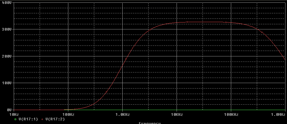
The two stages amplifier circuit as shown in the above figure indicates a feedback from the collector of the second bipolar junction transistor to the emitter of the first transistor. This is given to get fair values for the input and output resistances and better frequency responses. The noise intrusion and the distortions that happen to be mixed with the output are minimized. These are obtained with a slight lowering of the overall gain of the circuit. The simulation results of a two stages amplifier with feedback and without feedback are shown below.
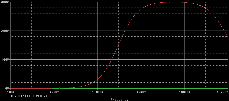
The above simulated output was obtained when a 100mv input was given. The output was observed as 300v. While the feedback was removed and simulation was carried out, the resulting output was about 325v.
Applying feedback always boosts the constancy of the amplifier. The characteristics of the circuit become linear with excellent frequency response. Though the gain is a bit lower, the other advantages are so bright that loss in gain is not considered.
The simulation of the circuit after removing the feedback loop resulted in an output as shown below. For an input of 100mv, the output turned out to be about 325v. This shows that the gain is higher compared to the two stages amplifier circuit with feedback loop. But, the stability of this circuit is lower than the circuit with feedback.
Comparison of Single and Two Stage Amplifiers
The insufficiency in gain of single stage amplifiers is removed by cascading more than one amplifier. If the gain obtained in a single stage amplifier is A, then the gain obtained by cascade of two such amplifiers is A*A. The efficiency is increased by adding number of stages. The output to a single stage amplifier is always shifted by 180 degrees with respect to the input, while a two stages amplifier output always is in phase with the input signal. The redundancies in the single stage circuit are almost eliminated in the case of two stages amplifiers, especially with feedback mechanism.
Digital Electronic House Alarm
Aim: To design a combinational and sequential digital electronic house alarm circuit.
Introduction
Intrusion alarm system is an electronic device which is used to identify the movement of the door. It uses the electronic and electrical property to monitor the mechanical movements. This circuit is designed using 7400 series and 4000 series family devices. When an intruder comes in by opening the door, the alarm is stimulated. The opening and closing of the door are the reason for the detection of intrusion. Separate circuits are assigned for each step of detection and conveyance of the trespass. Security is the major objective of our project. In recent days, the importance of security application is increasing, because of the increase in crimes.
Circuit Explanation
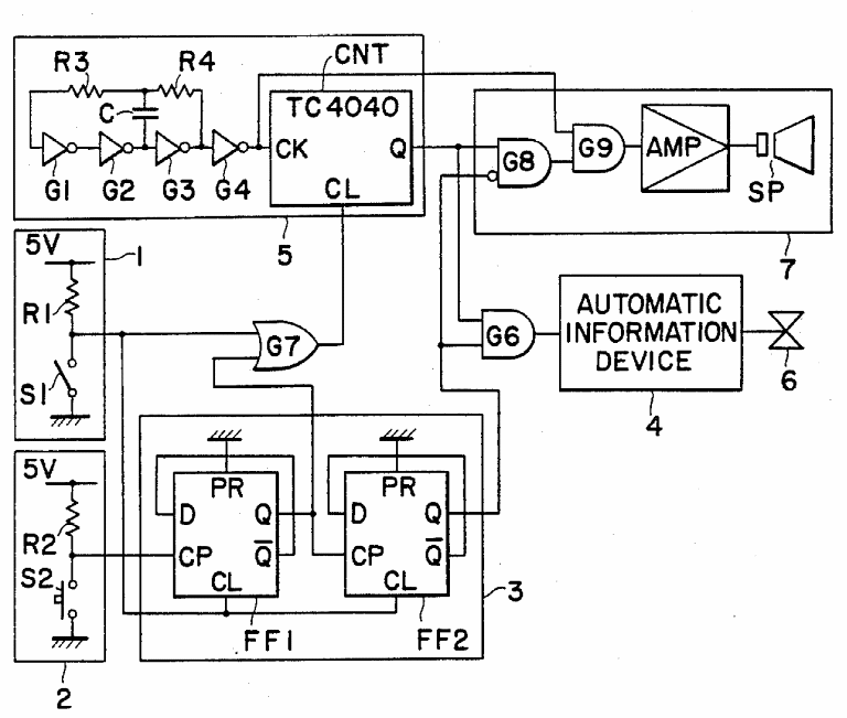
The circuit of intrusion alarm is given above. The alarm circuit comprises of combinational circuits and sequential circuits. The circuit of the intrusion detection and alarm system can be explained through the analysis of the circuit after dividing it into various parts. This makes the explanation easier and understandable.
The mode selecting circuit is indicated as 1 in the overall circuit diagram. It is shown separately below.
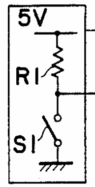
It consists of a resistor and a switch powered by a 5v supply. Open and close of the switch indicates the activation and deactivation of the system.
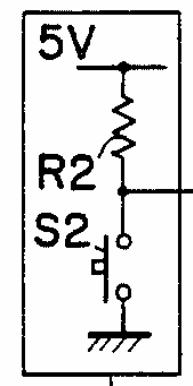
Block 2 is kept for the detection of the opened and closed state of the door. A door open detector runs a counter and the closure also initiates a timer which together detects the intrusion. This block consists of a simple circuit similar to that of block 1.
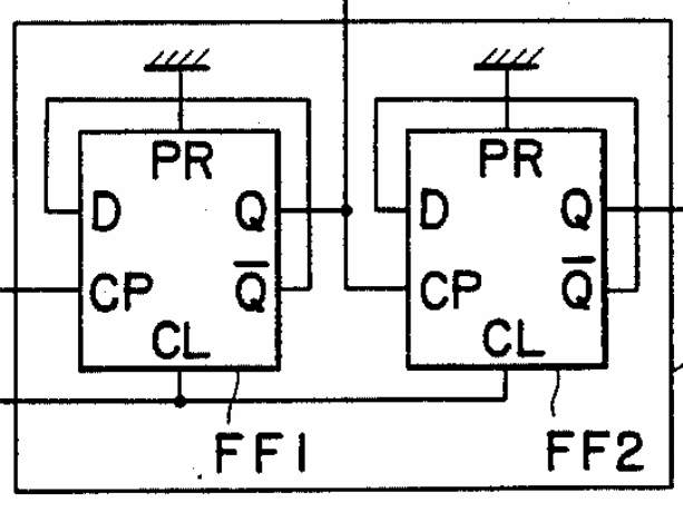
Block 4 is circuit for detecting the second time door opening. After setting the mode, the resident can go out by opening the door and closing it. This will not be detected as trespass. This block consists of two D flip-flops connected together. The Q bar output of the flip-flop is connected to its input D in both the flip-flops.
Block 4 is an automation device which informs the concerned place about the intrusion.
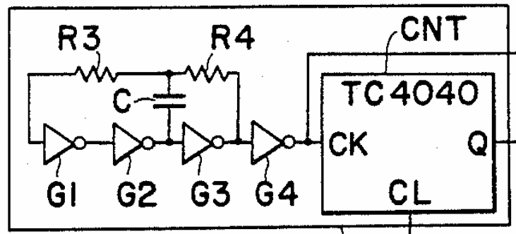
Block 5 shown above consists of an oscillation setup and a timer arrangement. The oscillator system produces the required frequency to the clock input of the timer circuit. Four invertors and two resistors with a capacitor are used to produce the oscillations. TC 4040 integrated circuit is used as a frequency divider timer. The timing of this helps in effective detection of intrusion. The second and subsequent door openings will set the timer on to reach a limit set by the resident. If the mode is changed within that stipulated time, the alarm will not be excited. Else, alarm is on to indicate a trespass.
The block 6 indicated in the overall diagram shows the communication line to the prescribed destination of conveyance of the detection.
Block 7 shown in the figure below specifies the arrangement for setting off the howling alarm.
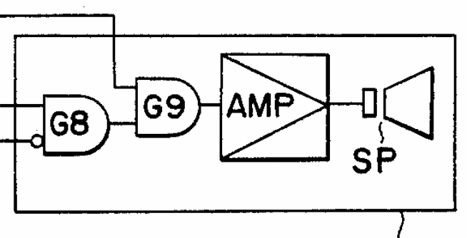
This comprises of two AND gates (G8 and G9) and an amplifier circuit connected to a speaker. One of the inputs to G8 is inverted whose output is given to G9. The output of G9 gives the stimulus for amplifier which outputs required power for driving the speaker.
Block 1 gives the clock input to block 3 and is also connected to one of the inputs of OR gate G7 whose output is the clock input to block 5. The second input to G7 is the Q output of the first flip-flop of block 3. G7 drives the counter to detect the intrusion. The Q output of the TC4040 and Q output of the D flip-flop 7474 are given to the G8 of block 7 where the D flip-flop output is inverted at the input of G8. Also, these are given to the AND gate G6 without any inversion whose resultant outcome drives the automation information block to inform the person via a communication line.
Thus, the circuit turns out to be built using simple components through simpler connections which are easy to analyze and absorb.
Working description
The system can be activated and deactivated by using the mode setting circuit indicated by 1 in the circuit diagram. When the owner goes out, the mode is activated. From that instance, a timer will start running. Before the timer runs out, the owner can go out by opening the door. As soon as timer times out, any opening or closing of the door will be detected as invasion. The intruder alarm includes the mode selection which has two modes.
They are ‘present’ mode and ‘absent’ mode. Present mode represents the presence of the resident in the house, buildings or office. In this mode, the intruder alarm will not be activated. The absent mode represents the absence of the resident in the house, buildings or office. In this absent mode, the intruder alarm will be activated by the resident himself/herself. The alarm detects whether the door is open or closed. If the resident is going out, the absent mode of the intruder alarm will be activated.
There may be some difficulties in this. To avoid such situation, a counter measure is also introduced. If the detection is made immediately after the mode settings, there is a chance to detect the presence of the resident which is incorrect. So, there will be a time interval between the mode setting and the final door closing. This is for the safety of the resident, i.e. when the alarm is set in absent mode; the circuit will activate and detect the trespass, only after a fixed time. This system will avoid the confusion. The creation of intruder alarm includes mode selection.
In the figure which is given above, the intruder alarm is shown. The mode setting is also explained in this figure. In this mode selection circuits, there are one pull up resistor R1 and one switch. In this figure, the mode selection part is represented as 1. The switch and the pull up resistor are collectively represented as 1. In this section, both the switch and resistor are connected serially and are connected to 5 V power source and other side is grounded as shown in the figure.
The output is taken from a common point of switch and pull up resistor. The output of the mode selection circuits leads to gate 7 and CLEAR pin (CL) of D flip-flop FF1 and FF2. The next one is the door open or close circuit which is used to detect whether the door is open or closed. In this section, the components are same as previous one, and here the resistor is R and the switch is S2 and all are serially connected and with power source of 5 V and other end is grounded same as in the mode selection section. The output of the door open close section is taken from the middle of the resistor and switch, and leads to the CP pin of the flip-flop FF1.
The both flip-flops are collectively known as the sequential circuit 3.The output Q of the FF1 leads to CP terminal of the FF2 and gate G7. The output Q bar leads as a feedback in its own input D terminal. In this, FF1 is the master flip-flop and FF2 is the slave flip-flop and present terminal of both flip-flops are grounded.
The sequential circuit 5 is the timer circuit. It comprises of counter and other four NOT gates or inverters G1, G2, G3, and G4. It includes the resistors R3 and R4 and a capacitor. The counter is included in the 4000 family. The output of the oscillator circuits that signal which has the known frequency, leads to the clock terminal CLK of the counter. Here, the input of the counter is the CLK terminal. The use of the counter is to divide the frequency for getting the desired time interval. When the mode selection sequential circuit is in the closed state, the input of OR gate G7 is in high state. So, the output of gate G7 will be high.
This leads to the clear terminal of the counter and both flip-flops. So, in the open state of the mode selection circuit, the alarm is in the present mode i.e. the circuit is idle in this state. If the mode selection circuit is closed, the power source is grounded and the output of the sequential circuit 1 will be low. So, the alarm circuit is in the absent mode i.e. the circuit is active. In the absent mode, the alarm circuit is vigilant for detecting the trespasser. In the absent mode, the switch in the door open close circuit is closed and the power source is grounded. So, the output to the sequential circuit is low and input to the input CP of flip-flop FF1 is low.
When the intruder opens the door in the absence of the resident, the switch in the sequential circuit 2 is open and its output is high. So, the D flip-flop is set and the output is high. The output of FF1 leads to the input of the FF2. So, FF2 is also set. So, the output of the FF2 is high. The output leads to the clear pin of the counter also. The FF2 output leads to the speaker. Here, use the 8 Ohm resistor instead of the speaker. Otherwise, one cannot calculate the simulation by using the PSpice. The timer circuit helps to make the time interval.
Simulation
For simulating the alarm circuit, the PSpice software is used here. ”SPICE is a powerful general purpose analogue and mixed-mode circuit simulator that is used to verify circuit designs and to predict the circuit behaviour.” (PSPICE, A Brief primer: Introduction 2006, 1).
It has great importance in designing and simulating the integrated circuits. There are many types of analyses. They are DC analysis which helps to calculate the DC transfer curve. The other one is non-linear transient analysis which helps to plot the voltage, current etc and Fourier analysis is used to analyze the frequency spectrum. Linear AC analysis calculates the output function of the frequency and it can be plotted and there are many others, such as, noise analysis, parametric analysis and Monte Carlo analysis. For designing the circuit, all components are available in the circuits. For getting simulation result, use the 8 ohm resistor instead of speaker. Here, one can check the voltage across the 8 ohm resistor.
Simulation of the intrusion detection circuit
The simulation of the circuit was done on PSpice 9.1 software. This software is used to examine proper working of analogue and digital circuits used in various applications. The ease in usage and simpler way to analyze the output make it acceptable widely.
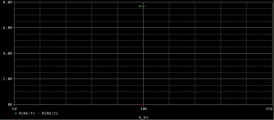
For the simulation of the intrusion circuit, the analysis settings were kept to DC Sweep because, only DC supply is present in the circuit. The outputs were observed at the ‘Present’ state, ‘absent with no intrusion’ state and ‘Absent with intrusion’ state. The simulation output result 1 and result 2 shown below indicate the ‘Present’ state and ‘Absent with no intrusion’ state. ‘Present’ state represents the inactivated scenario and ‘Absent with no intrusion’ state points to the situation where trespassing, that is opening of the door, is not being detected while the system is in activated mode itself.
The simulation output shown third is the output when an intrusion is detected. In the activated mode, if any intrusion is detected, the state is said as ‘Absent with intrusion’ state. The first two screen shots show 0v at the load while the third screen shot clearly indicates the voltage output sufficient to drive the load. The no-voltage at the load indicates that the speaker as well as the automation information block is idle and a voltage at the load represents that the alarm and the automation information system are at work.
Industrial application for intruder alarm
In the recent time, the importance of security system in every field is increasing. The intruder alarm also has many industrial applications. They are residential application or light application which can be explained here as the most common application used for the security of home and for commercial or industrial application. The intruder alarm circuit which is explained here is always suitable for home application i.e. door, window, or home itself. In our circuit, there is no wireless method for detecting the intruder. Here, only the open/close door sequential circuit is used which works according to the movement of door.
Review and Evaluation on two digital electronics device family
7400 series device family
“The 7400 series of Transistor-transistor logic integrated circuits are historically important as the first widespread family of TTL integrated circuit logic.” (7400 Series 2009).
This series consists of very primary level to higher level complex modules. They comprise of fate level integrated circuits to arithmetic and logic unit integrated circuits. There are entire range of gates like NOT, AND, OR, XOR, NAND, NOR, XNOR and flip-flops like D, T, JK, SR. counters. Bus transceivers are also present in this family besides the arithmetic and logical packages. The 7400 series devices are used in computers as well.
The ease in the usage of 7400 series family devices in the circuit finds its application in many fields. The circuit places where a fixed power supply can be set up with 7400 series integrated circuits. The main area of application is where speed limitation is not entertained. These circuits are always speedy in producing outputs than the 4000 series devices.
The examples of practical applications of the 7400 series family devices are the laboratory usages. In the field research and development of electro mechanical parts, the 7400 series of digital electronic circuit devices are used because of the ease in the analysis as well as the working pace. Since they are the basic family, it makes the designer to be able to evaluate them in circuits.
4000 series device family
“The 4000 series is a family of industry standard integrated circuits which implement a variety of logic functions using complementary metal oxide semiconductor technology.” (4000 Series 2009).
This family of digital devices was evolved to replace the 74 family devices. The power consumption in this family is lower compared to the 74 series devices. This multitalented family has brought a new phase of evolution in electronics, telecommunication and electro mechanical fields of technology. The speed constraints make the 4000 series devices a little backward. But, the circuit design is effortless in this case and also the input voltages are of a lengthier range than the 74 series device circuits. They are limited to fixed circuits unlike the 74 series circuit designs.
The use of 4000 series family devices in electromechanical field is extensively bigger. The low power consumption decreases the heat produced in the set up, thereby increasing the life time of the electromechanical parts of the system. Also, the supply needed to drive the mechanical parts is affordable by the 4000 series family digital electronics devices. These make them applicable in practical fields.
Example for practical implementation of 4000 series devices is their usage in building the electro mechanical parts in the Management and Implementation Plan for Space Station NASA. The following quotes from the plan imply its application in the plan: “Derating requirements imposed by SSP 30312 appendix B call for a 70% Derating factor on operating supply for CMOS 4000 series microcircuits. Since these devices have a maximum voltage of 20 Vcc, properly derated circuits should run at not higher than 14 Vdc.” (Electrical, electronic, and electromechanical (EEE) and mechanical parts management and implementation plan for space station program 1999).
The plan discussed above indicates that a variety of 4000 series devices are used in their implications in order to utilize the advantages like decreased consumption of power, wider voltage choice which enable an input voltage of about 14v.
Reference List
Educational kits: Amplifiers: Two stage RC coupled amplifier. T-Systems Electronics. Web.
Electrical, electronic, and electromechanical (EEE) and mechanical parts management and implementation plan for space station program 1999, NASA. P. 11. Web.
Intrusion alarm system with automatic exit control and misset indicator 2009, Free Patents Online: All the Inventions of the Mankind. Web.
PSPICE, A Brief primer: Introduction 2006, University of Pennsylvania Department of Electrical and System Engineering, Jvds. P.1. Web.
4000 Series 2009, AbsoluteAstronomy. Web.
7400 Series 2009, AbsoluteAstronomy. Web.