Introduction
Background
Nanotechnology is perhaps one of the fastest-growing sectors in the technological field. According to Berger (2010), it involves the study of and manipulation of matter on an atomic and molecular scale, which is very important in manufacturing and other industries. This technology also involves the development of materials and structures with at least one of its dimensions measuring between 1 and 100 nanometres (Berger 2010). The dimension, in this case, maybe the thickness of the device or structure been developed or its length.
Many scholarly articles have been written on the future of nanotechnology. The main interest of these articles and scholarly work is the effects- both negative and positive- that nanotechnology may have on humans. However, it is a fact beyond doubt that this technology can be used to come up with many new devices and materials that can be used in various fields in society. This is for example the application of nanotechnology in agriculture, medicine, chemistry, and electronics among others.
Despite its potential in various fields, nanotechnology has raised many concerns regarding its negative effects on humans and the environment. For example, according to Chourasia and Chopra (2010), concerns have been raised on the toxicity and other impacts that this technology may have on the environment. For example, what effects does the release of nanomaterials have on the environment? How will this technology affect the world economy? These are just some of the questions raised by the increased application of nanotechnology.
Most of these concerns are associated with the fact that nanotechnology is a fairly recent development in the technological world. As such, there are many aspects of the technology that are unknown, including the negative effects that it may have on humans. To address these concerns, government agencies and other stakeholders have realized the importance of regulating nanotechnology. As a result, activities involving this technology (such as experiments and production of nanomaterials) have to be sanctioned by the governments and other relevant authorities.
The Rise of Micro- and Nano- Engineering Industry
As already indicated in this paper, nanotechnology has been applied in many fields and industries around the world. Engineering is one field that has embraced nanotechnology.
Messina, Rivera, Olguin, and Ruiz (2002) regard nanoengineering as a form of engineering that is carried out on the nanoscale. The nanometre, after which this field is named, is a unit of measurement that is equal to a billionth part of a meter. Generally, nanotechnology is synonymous with pure sciences such as biology and chemistry. However, when applied in the field of engineering, the emphasis is more on the engineering aspect of this technology than on its pure science attributes (Messina et al 2002).
The rise of the nanoengineering industry has been associated with the increasing demand for devices with high precision. This is for example the demand for spaceship skins that can resist the effects of overheating as the spaceship enters the atmosphere. Others include the demand for surgical devices with increased precision to enhance surgical procedures.
Demand for Advanced Analytical Techniques in Nanotechnology: A Case Study of Nanoengineering
As the micro-and nano-engineering industry grows in leaps and bounds, there is an accompanying rise in demand for more advanced analytical and characterization techniques for the materials and systems that are used and produced in the process. This is especially so because nano-products are significantly different from their larger geometry counterparts, and as such require equally different techniques to analyze and handle them (Evans Analytical Group [EAG] 2007).
For instance, a nano-product that has a high surface-area-to-volume ratio has increased sensitivity during production and storage. The sensitivity of such a product to impurities and micro-contamination during processing means that the yield of the whole production process is affected (EAG 2007). Micro-contamination increases defects, and it is these defects that lower the production yield.
Take the example of a spaceship outer skin that has been micro-contaminated during production. This contamination might lead to a rough surface which increases the friction between the ship’s skin and the atmosphere during re-entry. This will in effect reduce the efficacy of the whole process of space exploration as it might damage the ship.
According to EAG (2007), advanced analytical techniques have for the longest time addressed issues such as the cleanliness of products, reliability of devices and contamination of the final product, and the final output of the production process among others. These are the same issues that affect nanoengineering today, and as such, advanced analytical techniques are needed to address them.
Advanced analytical techniques can be used on various aspects of nanoengineering such as the product itself and the production process. This means that the techniques can be used on the tools used during nanoengineering, or they can be used to analyze the final product of the process.
This report is a demonstration of the usage of advanced surface analytical techniques in the process of manufacture and reliability characterization of new nanotechnology materials. This author investigated nanoengineering, a scientific field, and developed experimental protocols using two advanced analytical techniques. This report will describe planning, data acquisition, interpretation, and modeling.
Two advanced analytical techniques were used in this investigation. These are Scanning Electron Microscopy (herein referred to as SEM) and Auger Electron Spectroscopy (herein referred to as AES). This report will provide demonstrations of these two advanced analytical techniques as characterization devices in nano-dimension in the field of nanoengineering. The strengths and weaknesses of these two techniques will be provided, as well as how these strengths and weaknesses can be exploited. The report will also include an analysis of the complementarity of the two advanced analytical techniques, and how this complementarity can be exploited.
Literature Review
Nano-Dimension Materials’ Characterisation
According to Goldstein (2003), nano-dimension materials’ characterization is critical in many manufacturing industries that use nanoengineering. This includes the production of semiconductors for the electronics, automotive, and aerospace industries. Many manufacturing industries are today tending towards smaller and lighter characteristics, creating the need for nano-dimension materials’ characterization.
Characterization of nanomaterials is important in improving product yield and functional reliability in nanoengineering (EAG 2007). It is one way of increasing the volume of production while reducing wastage. It also increases the confidence of consumers in the product, hence increasing demand.
Advanced Analytical Techniques in Nanoengineering
According to Grant and Briggs (2003), analytical techniques in nanoengineering should be consistent with the surface, volume, or region that is to be analyzed. This is given that nanoengineering involves surfaces and volumes that are small. This means that analysis of the low-density distribution of nano-particles should be carried out using an analytical tool with a corresponding analytical area.
Several analytical techniques can be used on surfaces of nanomaterials in nanoengineering. They include the following:
- Transmission Electron Microscopy (also known as TEM0
- Time of Flight Secondary Ion Mass Spectrometry (also known as TOF- SIMS)
- X-ray Diffraction (XRD) among others
Following is a brief analysis of each of these analytical techniques:
Transmission Electron Microscopy (TEM)
This form of microscopy involves the transmission of a beam of electrons through a very thin specimen (Gondran, Charlene, and Kisik 2006). The electrons so transmitted interact with the specimen as they go through it. This process results in the formation of an image that is then magnified and focused on an imaging device such as a film (Gondran et al 2006).
It is noted that the transmission electron microscope is preferred over a normal light microscope in nanoengineering. This is given the fact that it gives an image with a much higher resolution due to the small de Broglie wavelength electrons used (Chourasia and Chopra 2010). This being the case, the scientist can examine minute details of the surface such as a column of atoms.
In an experiment cited in EAG (2007), a group of visibly spherical nanoparticles was examined using TEM. After sonication of the particles in methanol and distribution on a transmission electron microscopy sample grid, it was observed that most of the particles were not spherical. A multitude of shapes that were not discernible under a light microscope was observed. The results of this experiment go a long way in showing the significance of TEM in nanoengineering.
Time of Flight Secondary Ion Mass Spectrometry
This is another advanced analytical technique that is used in nanoengineering. According to Adams, Vaeck, and Barrett (2005), this method involves the use of a pulsed ion beam which “peels off” molecules from the outermost surface of the specimen. The nano-particles are peeled off from atomic monolayers on the surface of the specimen. They are referred to as secondary ions, giving this technique its name.
The particles so obtained are then accelerated through what Swapp (2011) refers to as a flight tube. Their mass is then determined by gauging the time of flight, which is the amount of time taken by the particles to reach the detector.
This technique lacks the spatial resolution of techniques such as TEM which uses an electron beam (Goldstein 2003). But it contains very low information depth ranging between 10 to 20A. What this means is that the technique is capable of giving the examiner information about surfaces that are coated by materials in monolayers or less (EAG 2007). This aspect makes this technique very important in the field of nanoengineering given that it can detect low levels of molecular contamination on surfaces of specimens.
X-Ray Diffraction
X-ray diffraction is a form of X-ray scattering technique that is used in nanotechnology to examine surface properties of thin materials such as films (Goldstein 2003). It is used to get information regarding the crystallographic structure of such a surface, as well as its chemical and physical attributes. The idea behind this technique is the analysis of the intensity of the scattered x-ray beam that is focused on a sample.
In another experiment reported in EAG (2007), nanoparticles were subjected to an x-ray diffraction process to determine whether the crystallographic structure was similar to what was expected when the material was purchased. The experiment used a SiC whose particles’ size was in the range of 55 nanometres. It was found that the crystalline size of the primary phase differed from that of nanoparticles. It was also determined that most of the nanoparticles were made up of multiple crystallites, not a single one (EAG 2007). This is an indication of the fact that this technique is indispensable in the nanoengineering field given the need to analyze the surfaces of nanomaterials produced and used in the field.
Data Collection and Analysis
Data Collection
As earlier indicated in the introduction part of this paper, the major aim of this report is to show the contribution of advanced analytical techniques in the nanoengineering field. The paper aims to demonstrate how the techniques can be used as nano-dimensional characterization tools. Two techniques (Auger Electron Spectroscopy and Scanning Electron Microscopy) were used.
Samples for the Study
Several nanomaterials were needed for this experiment. The study settled for nanomaterials made of aluminum and copper deposited on silicon. A similar study using these materials was carried out by EAG (2007), and the current study aims to assess whether EAG’s study can be replicated.
However, there are some differences discernible between the current study and that by EAG (2007). For example, EAG did not analyze the use of Scanning Electron Microscopy, an aspect that will be incorporated in the current study.
Some considerations led to the selection of aluminum and copper deposited on silicon over other nanoparticles. One of them is the fact that the material is commercially available and easy to access as a source of nano-particles. As such, the material was simply obtained through a purchase made locally. Secondly, it was the material that was used in EAG (2007), and given that the current study intended to replicate the one by EAG, it was logical to use similar materials.
Analytical Techniques to be used
Before embarking on the analysis of the current study and the collection of data, it is important to provide a brief background on the two advanced analytical techniques that will be employed. These are scanning electron microscopy and auger electron spectroscopy. This background aims to enable the reader to locate the rest of the study within the larger field of advanced analytical techniques used in nanoengineering.
Auger Electron Spectroscopy
This technique involves the use of a high energy primary electron beam within the range of 2 to 10 keV (Egerton 2005). The sample to be studied is exposed to this beam, giving rise to a series of backscattered Auger electrons that are secondary (Goldstein 2003). The resulting electrons are then detected and analyzed. The electrons are then focused on an imaging surface, similar to the SEM process that will be analyzed below.
This technique is used to study surfaces especially in the nanoengineering field, and this is one of the reasons why it was selected for the current study. The energies of the resulting Auger electrons are discrete (Adams et al 2005), and they are a pointer to the elements that are deposited on the surface of the specimen (Egerton 2005). The peak positions of the Auger electrons are the ones that are analyzed to identify the elements present on the surface and their chemical composition.
Scanning Electron Microscopy
This method involves the use of a Scanning Electron Microscope (SEM) which operates on high-energy electrons (Messina et al 2002). A focused beam of these electrons gives rise to a multitude of signals on the surface of the sample specimen.
When the electrons interact with the surface of the sample, distinct signals are developed. Analyses of these signals provide information on the properties of the surface. This includes the texture of the surface, its crystallography, chemical composition, and other attributes of deposits on the surface.
Again, this technique was selected given the fact that it is mainly used in analyzing surfaces of samples, and this was the major aim of this paper.
Observations Made
The aluminum and copper nanoparticles were subjected to the two analytical techniques described above to assess their composition.
Results for Auger Electron Spectroscopy and Scanning Electron Microscopy
It was noticed that the AES technique gave rise to enhanced spatial resolution when compared to that of SEM. It had a higher surface sensitivity, and these conclusions are similar to those made in EAG (2007). This characteristic makes the two techniques highly complement each other.
To exploit the complementarity of the two techniques, the area of the sample that was used for Auger was also used for SEM imaging. The information depth of AES is usually within the range of 30 and 60A, enhancing its complementarity to SEM further.
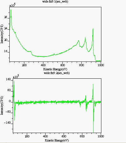
The figure below is a sample of an Auger Electron Spectroscopy spectrum of a copper grid. The image at the top represents the measured spectrum while the one below it is an indication of a derivative:
Individual nanoparticles were further subjected to elemental analysis and the results compared to those in EAG (2007). The results were comparable, and are presented below:
Elemental Analysis Results for Current Study
Aluminium: C (40%) Si (23) Al (20%) O (17.5%) Cu (0.4%)
Copper: C (38%) Si (27%) O (21%) Cu (14%)
Elemental Analysis Results for EAG (2007)
Aluminium: C (43%) Si (20%) Al (19%) O (18%) Cu (0.6%)
Copper: C (40%) Si (25%) O (19%) Cu (16%)
From the results above, it is clear that the study conducted by EAG (2007) is comparable to the current one.
Weaknesses and Strengths of the Techniques used
Scanning Electron Microscopy
One major weakness of Scanning Electron Microscopy is the fact that it can only be used on solid specimens (Swapp 2011). This means that it cannot be used to analyze the surface properties of gases and liquids. Another weakness is the fact that the size of the sample to be analyzed is limited. This is given the fact that the sample must be small enough to fit into the microscope chamber, meaning that large samples cannot be accommodated (Messina et al 2002). According to Swapp (2011), the microscope chamber can only accommodate a sample that is 10 centimeters long and 40 millimeters thick.
It is also noted that the specimen should remain stable in the vacuum chamber. This means that specimens such as coal and other organic materials that are unstable under low pressures cannot be analyzed using this technique (University of Alberta 2003).
These weaknesses were exploited given that the sample used in this study was solid aluminum and copper deposited on silicon. The sample could be scaled down to small sizes to fit into the chamber and it remained stable under low pressure.
The major strength of SEM is the fact that it is one of the most effective ways to analyze the surfaces of solid materials. This is the reason why it is highly applicable in geology and nanoengineering. The data is also acquired within a short time, usually less than five minutes. The sample does not have to be elaborately prepared to be examined, and the resulting image can be digitized, making it highly portable. These strengths were exploited and this is the reason why SEM was selected for this study.
AES
One major weakness of this technique is the fact that it can only analyze conducting and semi-conducting specimens such as metal (Chourasia and Chopra 2010). Non-conducting specimens have to be processed before they are subjected to AES. This includes coating a specimen such as a spider with gold before putting it under an AES machine. Like SEM, this technique is also used on solid specimens only. Additionally, specimens that are unstable under an electron beam are not suitable for this procedure. It is also not possible to quantify data from AES. These weaknesses were exploited given that the sample used in this study was solid, conducting, and stable under an electron beam. For quantification purposes, SEM was used as a compliment.
A major strength of this technique is the fact that it can be used to analyze almost any solid specimen provided that it remains stable under an electron beam and it can conduct. This technique can analyze the specimen as it is, meaning that special preparations are not needed. However, given that the analysis is carried out in a high vacuum, there is a need to clean the surface of some of the specimens before they are put in the vacuum chamber. The analysis also takes a short time given that a survey spectrum can be obtained in less than five minutes (Swapp 2011). These strengths were also exploited and that is the reason why the aluminum and copper sample was used.
References
Adams, F Vleck, L V and Barrett, R 2005. Advanced Analytical Techniques: Platform for Nano Materials Science, Spectrochimica Acta Part B Atomic Spectroscopy, 60(1); 13-26.
Berger, M 2010. Nanotechnology and the Future of Advanced Materials, Web.
Chourasia, A R and Chopra, D R 2010. Handbook of Instrumental Techniques for Analytical Chemistry, Texas: Texas University Press.
Egerton, R F 2005. Physical Principles of Electron Microscopy: An Introduction to TEM, SEM, and AEM, London: Springer.
Evans Analytical Group [EAG] 2007. Analytical Methods for Nanotechnology, Web.
Goldstein, J 2003. Scanning Electron Microscopy and X-ray Analysis, London: Kluwer Academic.
Gondran, C F Charlene, J and Kisik, C 2006. Front and Back Side Auger Electron Spectroscopy Depth Profile Analysis to Verify an Interfacial Reaction at the HfN/SiO2 Interface, Journal of Vacuum Science and Technology, 24(5); 24-57.
Grant, J T and Briggs, D 2003. Surface Analysis by Auger and X-Ray Photoelectron Spectroscopy, Chichester: IM Publications.
Messina, A R Rivera, S C Olguin, S D and Ruiz, V D 2002. Development of Advanced Analytical Techniques for the Analysis of Subsynchronous Torrsional Interaction with FACTS Devices, Electric Power Engineering, 2002.
Swapp S 2011. Scanning Electron Microscopy (SEM), University of Wyoming, 2011.
University of Alberta 2003. Auger Electron Spectroscopy, Web.